- 您现在的位置:买卖IC网 > Sheet目录3832 > PIC18F2520-I/ML (Microchip Technology)IC PIC MCU FLASH 16KX16 28QFN
2011-2012 Microchip Technology Inc.
Preliminary
DS41579C-page 387
PIC16(L)F1782/3
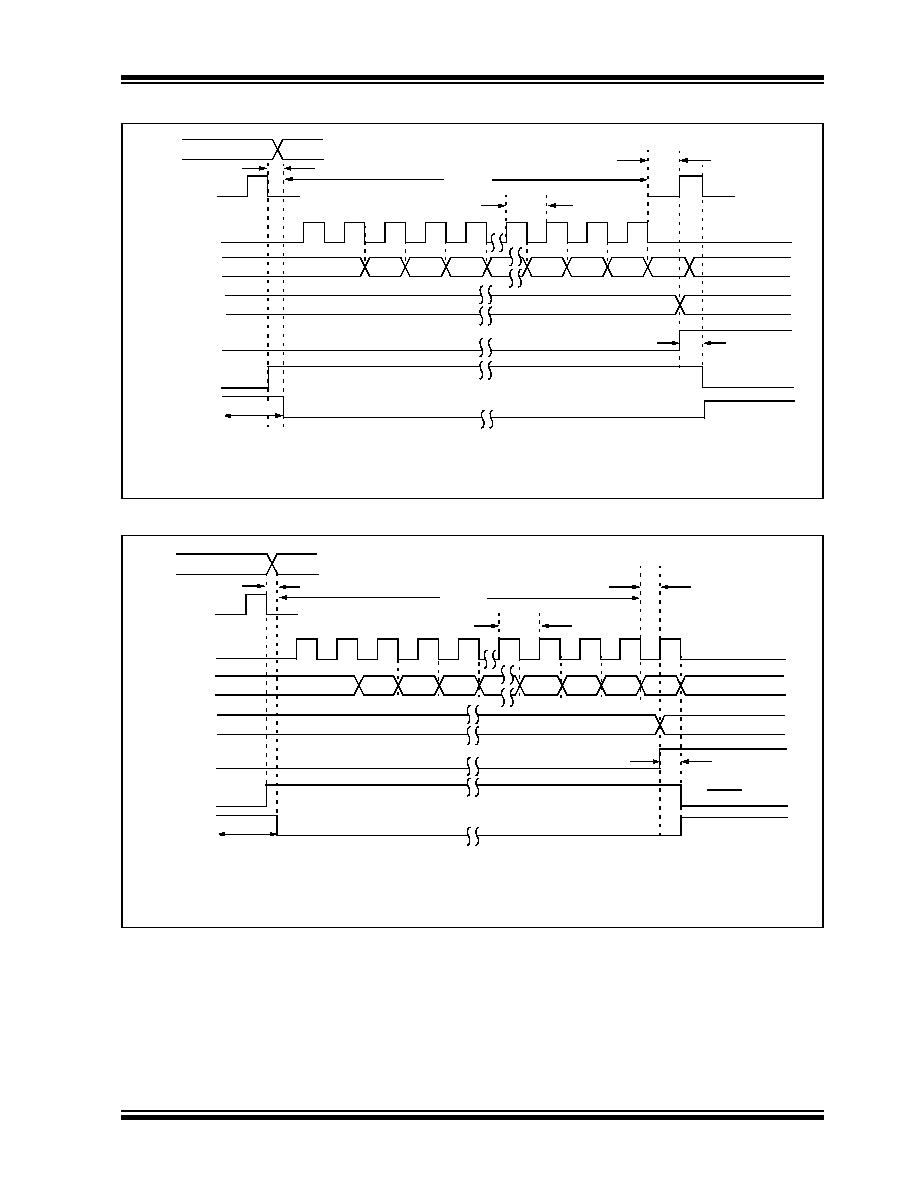
FIGURE 30-12:
PIC16(L)F1782/3 A/D CONVERSION TIMING (NORMAL MODE)
FIGURE 30-13:
PIC16(L)F1782/3 A/D CONVERSION TIMING (SLEEP MODE)
AD131
AD130
BSF ADCON0, GO
Q4
A/D CLK
A/D Data
ADRES
ADIF
GO
Sample
OLD_DATA
Sampling Stopped
DONE
NEW_DATA
76
5
3
2
1
0
Note 1:
If the A/D clock source is selected as RC, a time of TCY is added before the A/D clock starts. This
allows the SLEEP instruction to be executed.
1 Tcy
4
AD134
(TOSC/2(1))
1 Tcy
AD132
AD131
AD130
BSF ADCON0, GO
Q4
A/D CLK
A/D Data
ADRES
ADIF
GO
Sample
OLD_DATA
Sampling Stopped
DONE
NEW_DATA
7
5
32
10
Note 1:
If the A/D clock source is selected as RC, a time of TCY is added before the A/D clock starts. This
allows the SLEEP instruction to be executed.
AD134
4
6
1 Tcy
(TOSC/2 + TCY(1))
1 Tcy
发布紧急采购,3分钟左右您将得到回复。
相关PDF资料
AT87C51RC2-SLSUL
IC 8051 MCU 32K OTP 30MHZ 44PLCC
AT87C51RC2-RLTUM
IC 8051 MCU 32K OTP 40MHZ 44VQFP
AT87C51RC2-RLTUL
IC 8051 MCU 32K OTP 30MHZ 44VQFP
213684-4
34 PLUG KIT,M-SER,CC,JS,W/HOOD
202515-3
CONN PLUG BLOCK 42POS BLUE
202515-2
CONN PLUG M-SERIES 42POS
AT87C51RB2-RLTUL
IC 8051 MCU 16K OTP 30MHZ 44VQFP
AT87C51RB2-3CSUM
IC 8051 MCU 16K OTP 40MHZ 40DIP
相关代理商/技术参数
PIC18F2520-I/ML
制造商:Microchip Technology Inc 功能描述:8-Bit Microcontroller IC
PIC18F2520-I/SO
功能描述:8位微控制器 -MCU 32KB 1536 RAM 25I/0 RoHS:否 制造商:Silicon Labs 核心:8051 处理器系列:C8051F39x 数据总线宽度:8 bit 最大时钟频率:50 MHz 程序存储器大小:16 KB 数据 RAM 大小:1 KB 片上 ADC:Yes 工作电源电压:1.8 V to 3.6 V 工作温度范围:- 40 C to + 105 C 封装 / 箱体:QFN-20 安装风格:SMD/SMT
PIC18F2520-I/SP
功能描述:8位微控制器 -MCU 32KB 3968 RAM 25I/O RoHS:否 制造商:Silicon Labs 核心:8051 处理器系列:C8051F39x 数据总线宽度:8 bit 最大时钟频率:50 MHz 程序存储器大小:16 KB 数据 RAM 大小:1 KB 片上 ADC:Yes 工作电源电压:1.8 V to 3.6 V 工作温度范围:- 40 C to + 105 C 封装 / 箱体:QFN-20 安装风格:SMD/SMT
PIC18F2520T-E/SO
功能描述:8位微控制器 -MCU 32KB Flash 1536RAM 23I/O RoHS:否 制造商:Silicon Labs 核心:8051 处理器系列:C8051F39x 数据总线宽度:8 bit 最大时钟频率:50 MHz 程序存储器大小:16 KB 数据 RAM 大小:1 KB 片上 ADC:Yes 工作电源电压:1.8 V to 3.6 V 工作温度范围:- 40 C to + 105 C 封装 / 箱体:QFN-20 安装风格:SMD/SMT
PIC18F2520T-I/ML
功能描述:8位微控制器 -MCU 32KB 3968 RAM 25I/O RoHS:否 制造商:Silicon Labs 核心:8051 处理器系列:C8051F39x 数据总线宽度:8 bit 最大时钟频率:50 MHz 程序存储器大小:16 KB 数据 RAM 大小:1 KB 片上 ADC:Yes 工作电源电压:1.8 V to 3.6 V 工作温度范围:- 40 C to + 105 C 封装 / 箱体:QFN-20 安装风格:SMD/SMT
PIC18F2520T-I/SO
功能描述:8位微控制器 -MCU 32KB 3968 RAM 25I/O RoHS:否 制造商:Silicon Labs 核心:8051 处理器系列:C8051F39x 数据总线宽度:8 bit 最大时钟频率:50 MHz 程序存储器大小:16 KB 数据 RAM 大小:1 KB 片上 ADC:Yes 工作电源电压:1.8 V to 3.6 V 工作温度范围:- 40 C to + 105 C 封装 / 箱体:QFN-20 安装风格:SMD/SMT
PIC18F2523-E/ML
功能描述:8位微控制器 -MCU 32KB FL 1536bytes- RAM 25I/O RoHS:否 制造商:Silicon Labs 核心:8051 处理器系列:C8051F39x 数据总线宽度:8 bit 最大时钟频率:50 MHz 程序存储器大小:16 KB 数据 RAM 大小:1 KB 片上 ADC:Yes 工作电源电压:1.8 V to 3.6 V 工作温度范围:- 40 C to + 105 C 封装 / 箱体:QFN-20 安装风格:SMD/SMT
PIC18F2523-E/SO
功能描述:8位微控制器 -MCU 32KB FL 1536bytes- RAM 25I/O RoHS:否 制造商:Silicon Labs 核心:8051 处理器系列:C8051F39x 数据总线宽度:8 bit 最大时钟频率:50 MHz 程序存储器大小:16 KB 数据 RAM 大小:1 KB 片上 ADC:Yes 工作电源电压:1.8 V to 3.6 V 工作温度范围:- 40 C to + 105 C 封装 / 箱体:QFN-20 安装风格:SMD/SMT